The Kempston joystick interface

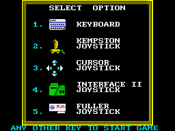
In the 80s, everyone who was a serious ZX Spectrum nerd had the Kempston joystick interface. If you were unfortunate enough that your parents bought you some Protek, DK'Tronix or (horrors!) Interface II nonsense, you kept quiet about it: that kind of gear would get you laughed off the playground. Possibly only the ComCon – with it's weird built in switchboard – could trump it, and nobody had one of those.
If you were a rich kid, you had the iconic Competition Pro, and the less well-heeled generally had a Quickshot II. You bragged about the autofire, but deep down you knew that the Competition Pro's microswitches were the GOAT. Parents a bit la-la? You probably had to endure the wrist-shattering Konix SpeedKing.
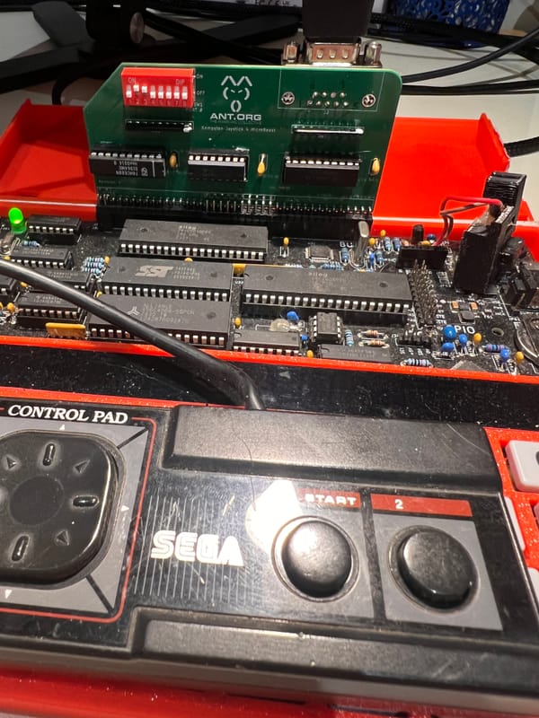
The Kempston interface itself cost £15 (about £68 in today's money), and you can build your own for about £15 today! I'll be building a Kempston compatible joystick interface for my trusty Feersum MicroBeast, but this should work for any retro system with an RC2014 backplane.
What's in a joystick?
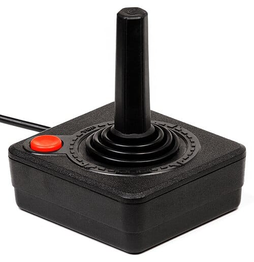
The classic 9-pin joystick of this era originated with the Atari VCS (2600) home games console, which came with stiff, square, minimalist sticks:
The 9-pin connector had a "common" pin that was connected to the fire button or any of the 4 principal directions as you pressed the button or moved the stick:
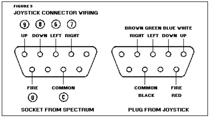
Note that the "common" pin is not specified as "ground". There were at least 4 revisions of the Kempston Joystick interface PCB, and the earlier ones used clever cost-reduction tricks which involved "common" being 5v, not ground, as was the de-facto standard at the time. This meant that joysticks with built in auto-fire hardware didn't work, as they were expecting 5v on pin 7 and ground on pin 8. (See this Tynemouth Blog article for fascinating details of these earlier versions).
What's in the joystick interface?
Surprisingly little! Here's the schematic:
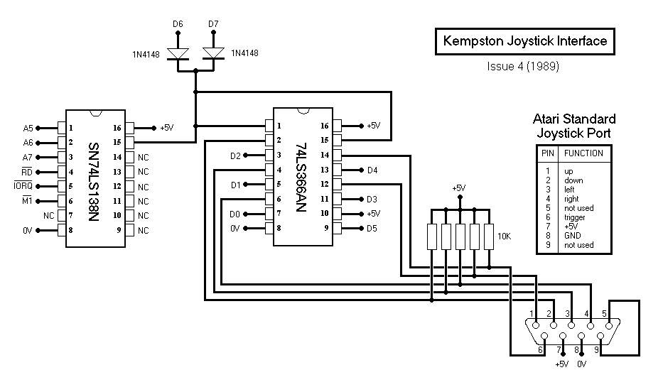
The joystick connector is bottom right, the common pin is ground or 0v in this revision, and all the joystick connections are "pulled up" to 5v via that bank of 5 10k resistors. This means that the signals from the joystick are 5v in their quiescent state, dropping to 0v when you press the fire button or move the stick.
These lines all go to 74LS366AN chip: this is a hex inverting buffer: buffer means a little amplifier to give the signal more oomph, inverting means that it outputs 0v when its input is 0v (and vice versa), and hex simply means that there are 6 of them on the chip. The inputs are all connected to the joystick, and the outputs are labelled D0, D1, ..., D5, which are the signals that make up the data bus on the Spectrum edge connector or the RC2014 backplane.
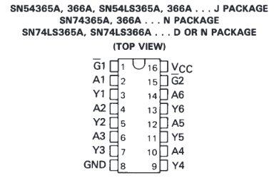
The inverting nature of the chip ensures that when a joystick signal goes low (i.e. is pulled to 0v by pressing fire/moving the stick) the corresponding data line goes high (5v) - in other words when your Z80 does an IN instruction to read this joystick interface's IO port (31 is the classic Kempston joystick port), it will see a 1 bit for switches that are currently active and a 0 bit for all others.
If you've a keen eye you might spot that there are 5 joystick signals, 6 channels on the 74LS366N, but 8 bits on the data bus. D0, D1, D2, D3, and D4 are used for the actual joystick inputs, and D5 is always low (0v): it comes from pin 9 on the chip (the Y4 output) whose corresponding input A4 (pin 10 on the chip), which is tied directly to 5v. 5v (HIGH) inverted => 0v (LOW).
We've run out of channels on the hex inverter, but we still have D6 and D7 to deal with. The designers could have left these floating, in which case the contents of these bits would have been random. Well designed games would mask out these bits before testing the real joystick inputs, but there was plenty of shoddy software out there that did a straight comparison, so these two unused bits needed to be consistent. Instead of going to the expense of using another hex inverter just to handle the two unused lines, we have the cunning diode-logic bus driver circuit formed by the two diodes at the top of the picture. More details later, but suffice to say that these two cheap diodes ensure that D6 and D7 are always low (0v).
Address decoding
You don't want to be driving the data bus with your joystick data all the time, otherwise your z80 is going to have a hard time getting anything useful done. The trick is to only put our joystick info on the bus when the z80 specifically asks for it, which it will do by issuing an IN instruction to read the provided 8-bit IO port address. All the address lines are available to us, so we can use them to match four different conditions:
- our IO port address appears in address lines A0 to A7
- the
R̅D̅line is low, meaning that the z80 is trying to read something - the
I̅O̅R̅E̅Q̅line is low, meaning that the z80 is accessing the IO (peripheral) bus - the
M̅1̅signal is high, meaning it's an IO request and not an "interrupt acknowledgement", which is the other legitimate reason for the previous 3 conditions being true
The G1 and G2 pins on the 74LS366N are the "output enables" - when these are low, the hex inverter drives the data bus with the joystick information, and when they're high it is effectively disconnected from the data bus.
These two pins are connected to the other chip, the SN74LS138N. This is a "3 line to 8 line decoder", and it is very commonly used for address decoding duties as it's a very versatile, Swiss Army knife of a chip.
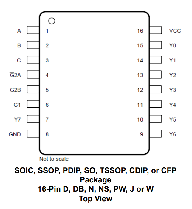
Those Y pins are all outputs, and precisely one of them goes low (0v) at any given time.
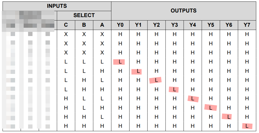
The currently low line is determined by the inputs A, B and C, which form a simple 3-bit binary address that selects the active (low) output. So if A, B, and C are all low, that's binary address 000 or 0 in decimal, so line Y0 is the only one that is active (low, 0v). If A, B, and C are all high, that's binary address 111 or 7 in decimal, so line Y7 is the only one that is active (low, 0v).
Once all the pins for the above features are allocated there are three left over, so the chip's designers made the genius decision to give the chip three separate enable signals, two active low and one active high, so the above picture becomes:
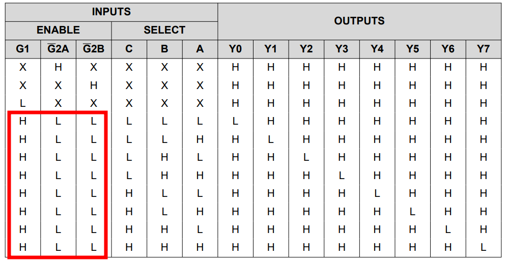
G1 must be high, and G̅2A must be low, and G̅2B must be low for the chip to activate: any other combination causes all its outputs to be inactive.
All of which means that this single, versatile, cheap component can be used to do address decoding for 6 different input signals. That's precisely what's going on in the Kempston schematic: we're using the Y0 output from this chip to drive the output enable pins of the hex inverter chip.
Also note that Y0 is connected to the bottom of those two diodes we discussed earlier. This means that they'll only drive D6 and D7 low when the interface is correctly addressed.
We can see that the M̅1̅ signal goes to G1 (must be high), the I̅O̅R̅E̅Q̅ signal goes to G̅2B (must be low), and the R̅D̅ goes to G̅2A (must be low), so that's the all of our secondary signalling taken care of... what about matching the IO port address? Well, we can see that the chip's A, B, and C inputs come from A7, A6 and A5, three of the system's address lines, which doesn't seem like enough!
IO port address space is 8 bits wide, not the full 16, so we can ignore A8 to A15, but we still ought to be decoding A4 through A0! However, the Kempston joystick doesn't bother, meaning that it will respond to any IN read where the IO port has the top 3 bits low. So that's 31 (0x1F) sure, but also 30, 29, 28, 27... and so on. This is known as a partial address decode or incomplete address decode and was incredibly common because it helped to keep costs down. As long as you avoided clashing with any internal hardware you'd get away with it. The problems came when two external peripherals both using the same cost-saving trick were connected at the same time. This was thankfully rare, and you'll note that the Kempston joystick interface does not have a pass-through connector.
Now that we understand the circuit, we can crack on with building our own equivalent, but we'll push the boat and do full address decoding, because you're much more likely to see other peripherals on an RC2014 bus. Join me in part 2 to get started!

Comments